 40G/100G Optical Transceivers
 25G Optical Transceivers
 10G Optical Transceivers
 155M/2.5G Optical Transceivers
 1G Optical Transceivers
 1G BIDI Optical Transceivers
 Dual-Rate Optical Transceivers
 FC 16G/32G Optical Transceivers
 CWDM Optical Transceivers
 DWDM Optical Transceivers
 SGMII Port Optical Transceivers
 XFP Optical Transceivers
 100M/1G/10G Coppers
 Full-Rate AOC & Breakout Series
 10G/40G Active DAC Series
 Full-Rate Passive DAC Series
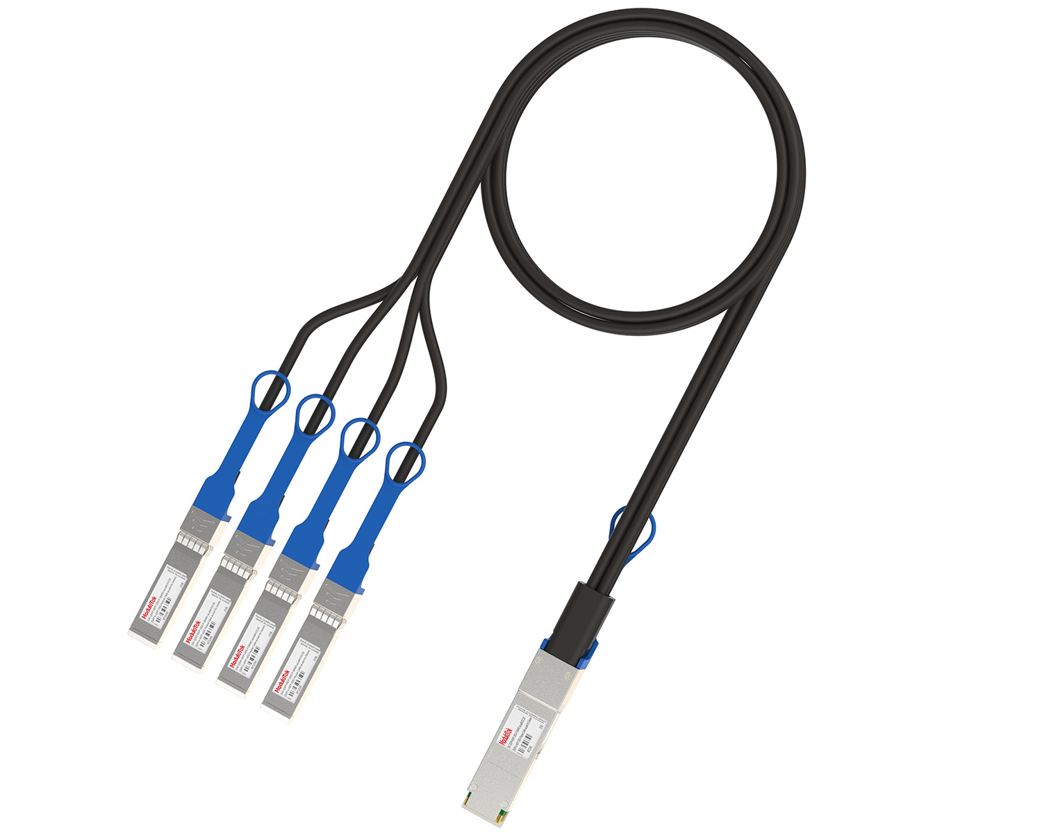 40G/100G Passive Breakout DAC Series
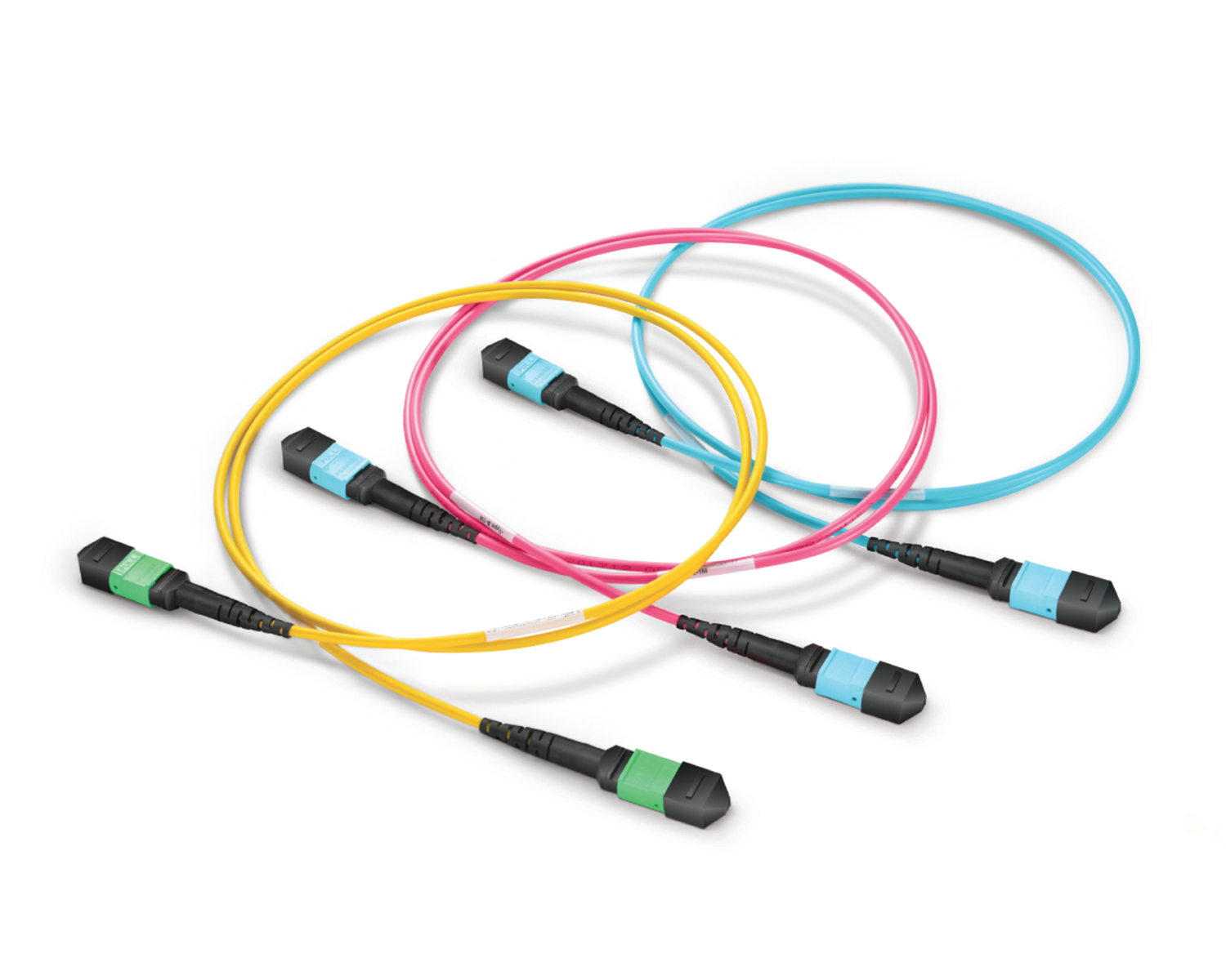 Regular/MTP-MPO Fiber Patch Cords
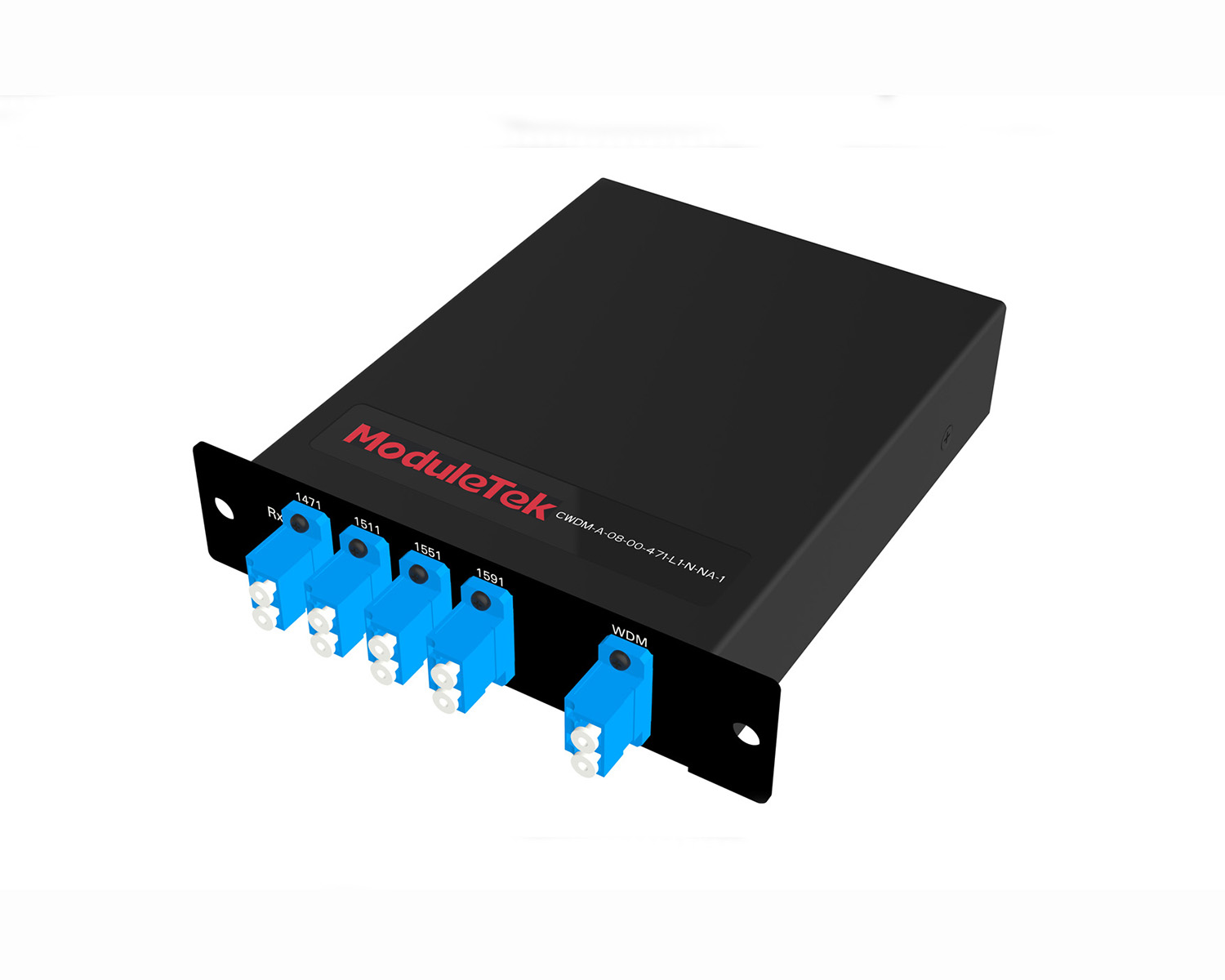 MT2011
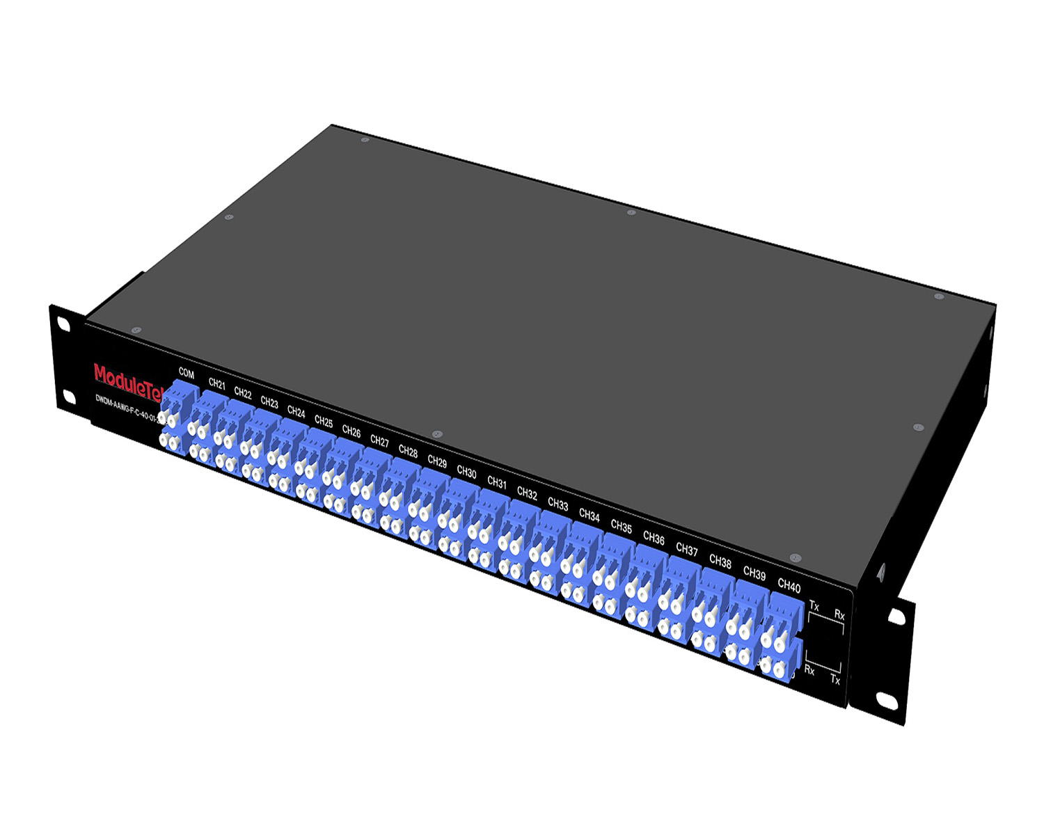 MT2010
 CodingBox
 QSFP to SFP Adapter
Teardown of Nokia 7250 IXR-e Switch
Time: 2024-03-05
Moduletek Laboratory recently purchased a Nokia 7250 IXR-e switch (24SFP+ 8SFP28 2QSFP28). We previously shared its unboxing in the article Nokia 7250 IXR-E Switch Unboxing. To further understand this device, we perform a basic teardown and analysis to showcase its internal structure.
Device specifications and panel interface details have been introduced earlier and will not be repeated here.
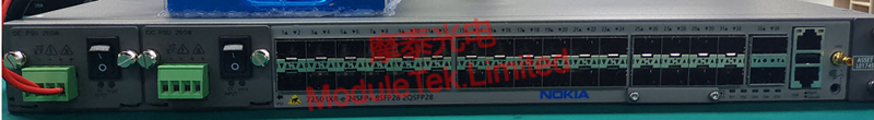
Figure 1 Nokia 7250 IXR-e Front Panel
After removing the top cover, the internal structure is divided into two main parts: a main PCB control board integrating various chips, resistors, and heat dissipation components; and a power board connected with two external DC power modules. Four cooling fans are independently mounted on one side.
The main PCB features one Altera 5M2210ZF324C4N (MAX V CPLD) chip of the same model on both its front and rear sides. Next to the power module is the memory bank, which contains 9 Samsung K4A4G08WF-BITD memory chips. A vertical metal baffle is installed between the memory chips and the CPLD. Beneath the largest heat sink are four parallel Samsung K4A4G165WE-BIRC memory chips, with a Marvell 88E1512-NNP2 Gigabit Ethernet transceiver adjacent to them.
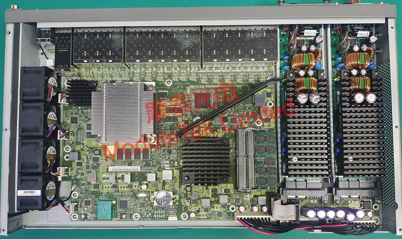
Figure 2 Internal Structure of Nokia 7250 IXR-e
The rear side of the main PCB has a dense layout of solder points, reflecting a highly integrated circuit design.

Figure 3 Rear Side of Nokia 7250 IXR-e Main PCB
After removing the largest heat sink, the main switching chip is exposed: a Broadcom BCM88470CB0IFSBG. The other two black heat sinks are tightly bonded to the underlying chips, so we do not forcibly remove them during this teardown.
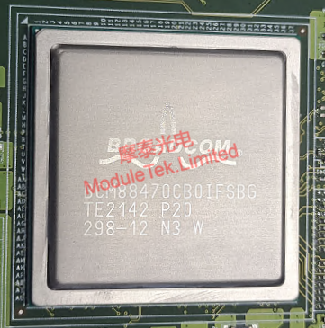
Figure 4 Main Switching Chip of Nokia 7250 IXR-e
After teardown, reassemble the switch and reboot it to check the system status. The normal startup of the sleek TIMOS operating system indicates the device is in good working condition.
Moduletek sincerely serves you.
For further inquiries about the above content, please contact us at: sales@moduletek.com


