 40G/100G Optical Transceivers
 25G Optical Transceivers
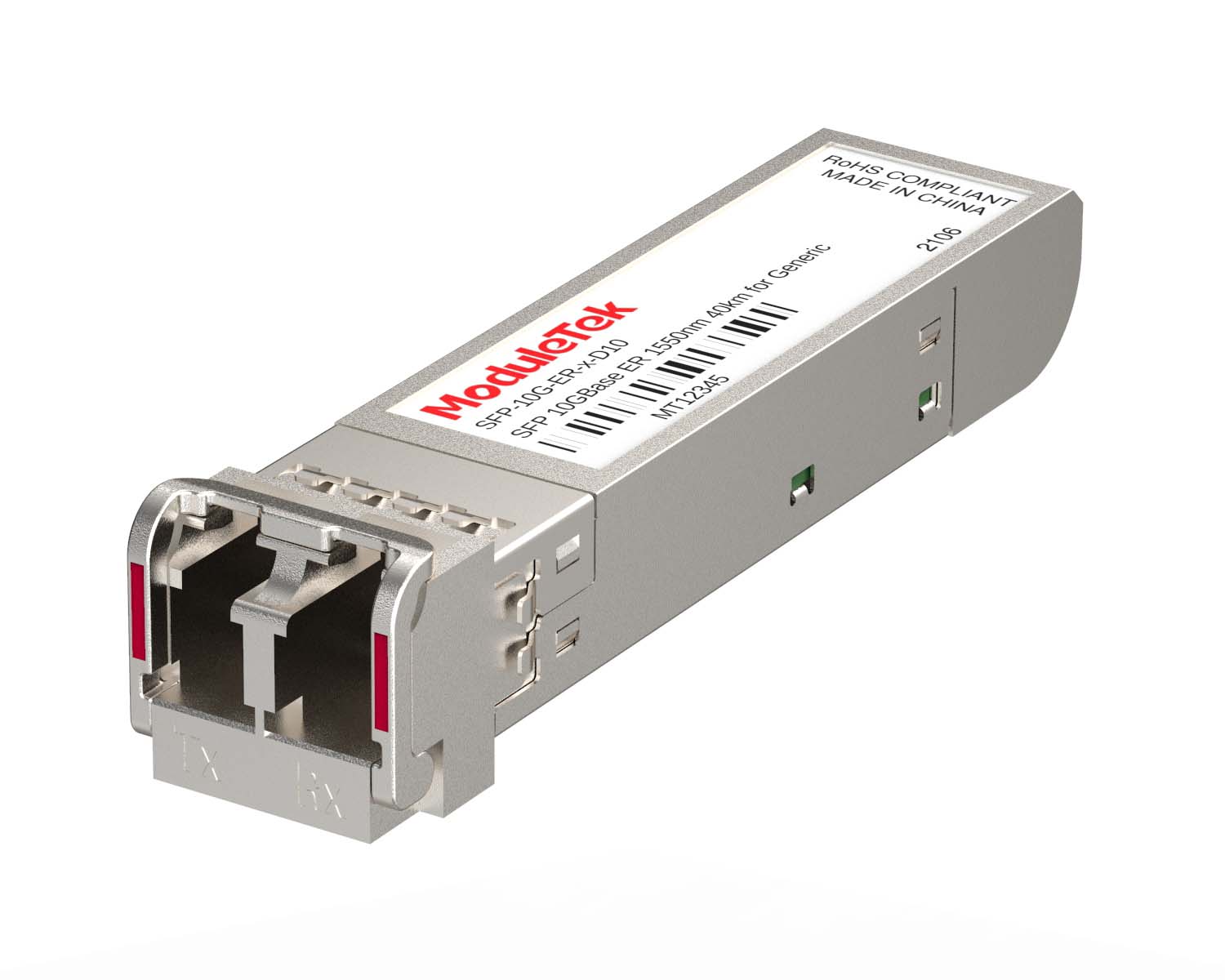 10G Optical Transceivers
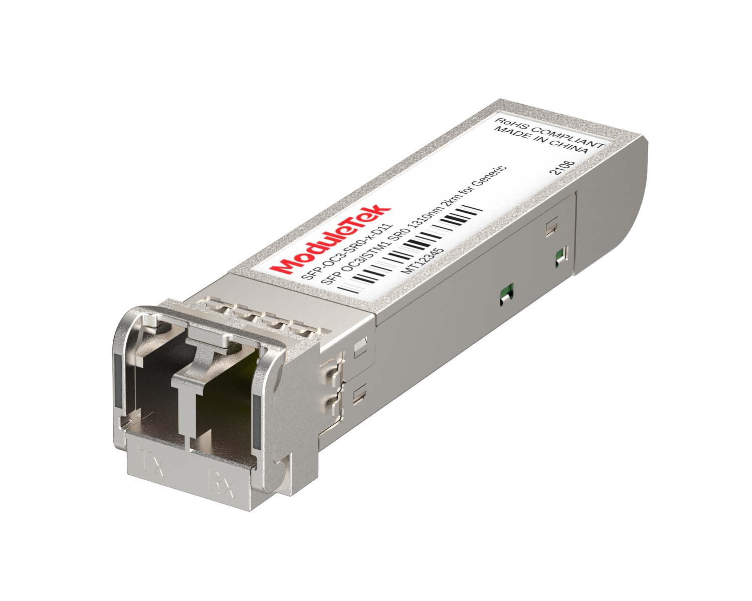 155M/2.5G Optical Transceivers
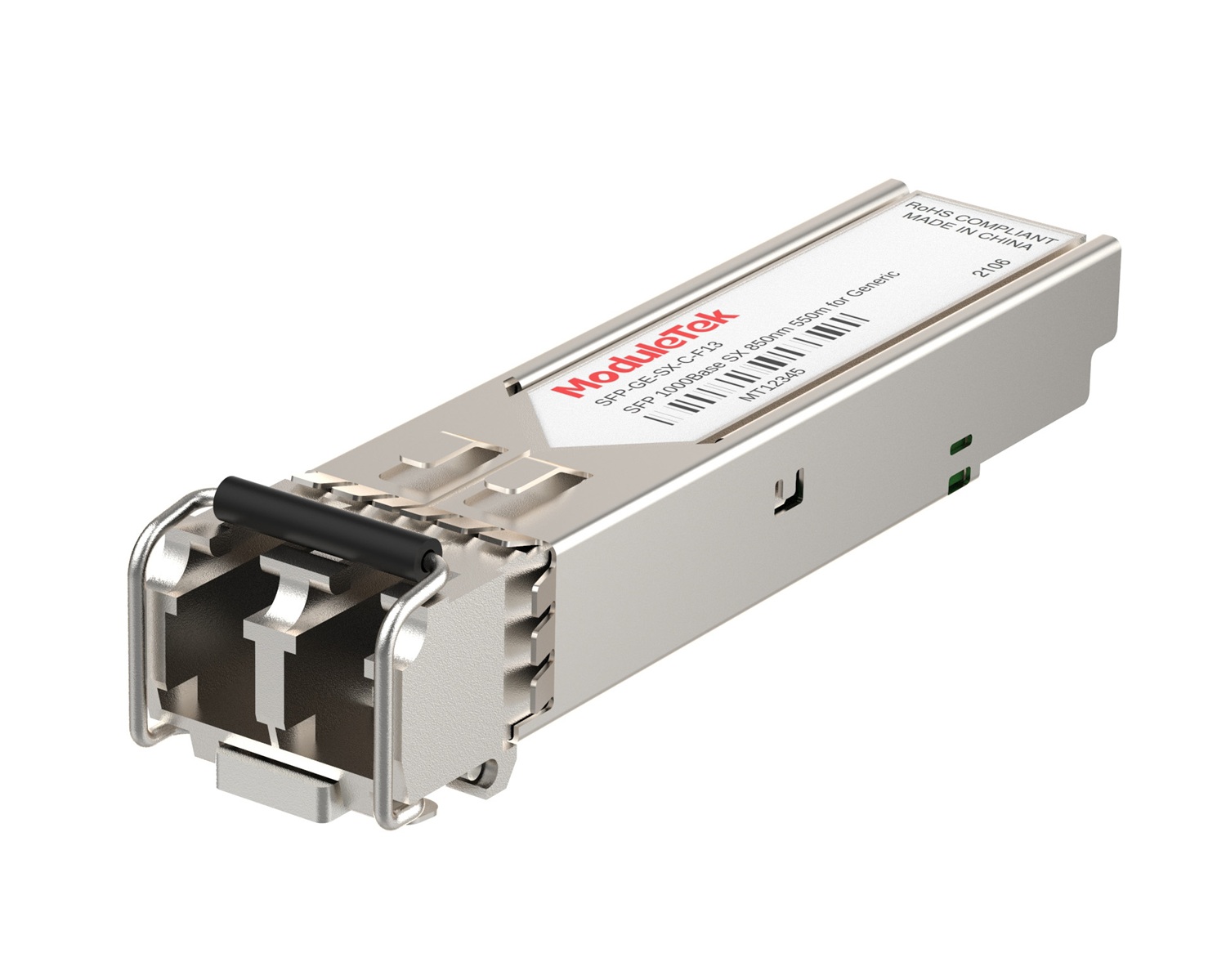 1G Optical Transceivers
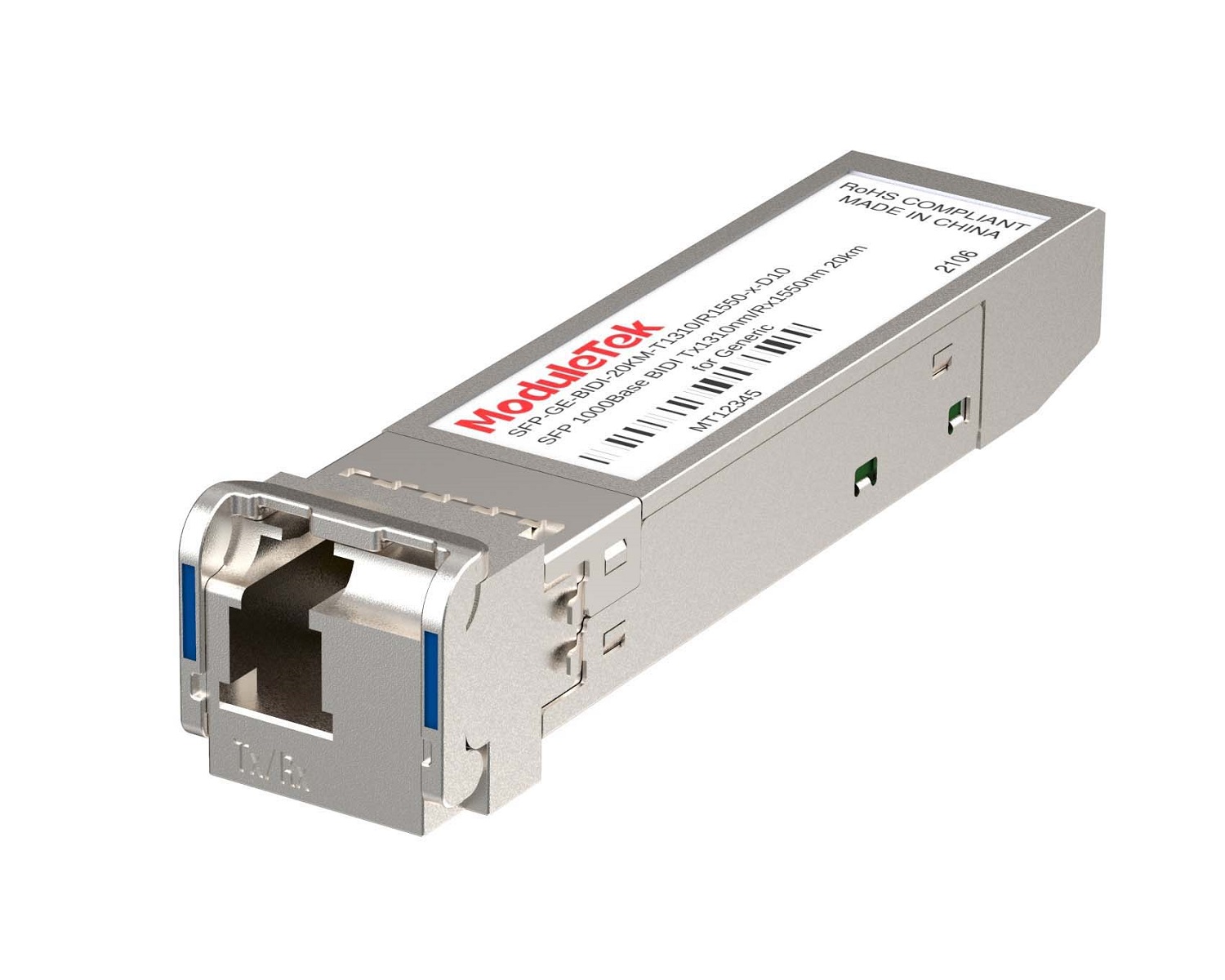 1G BIDI Optical Transceivers
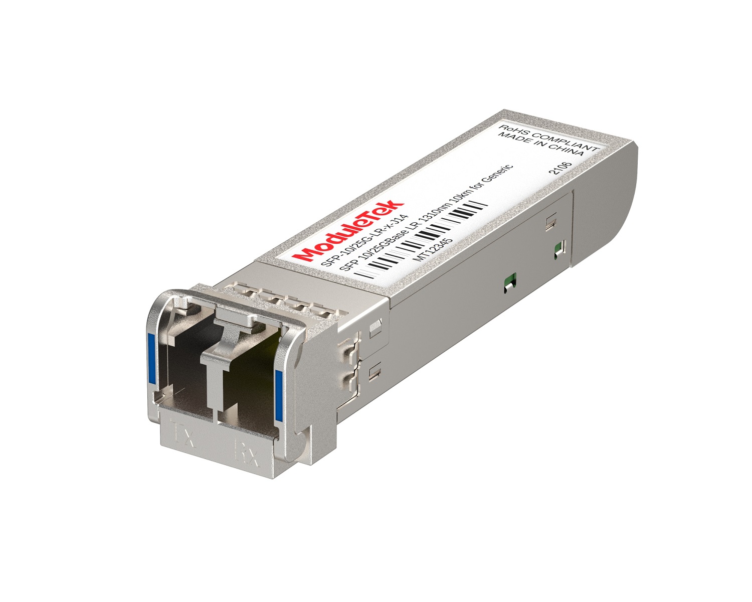 Dual-Rate Optical Transceivers
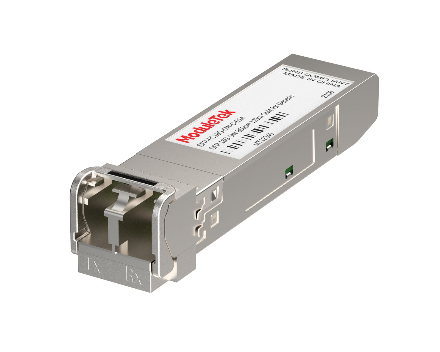 FC 16G/32G Optical Transceivers
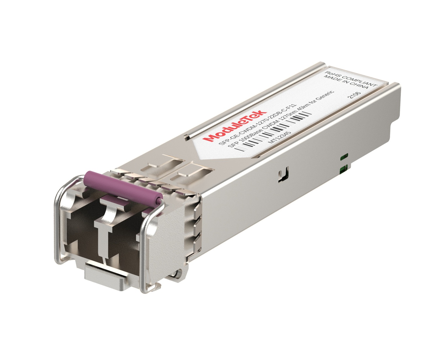 CWDM Optical Transceivers
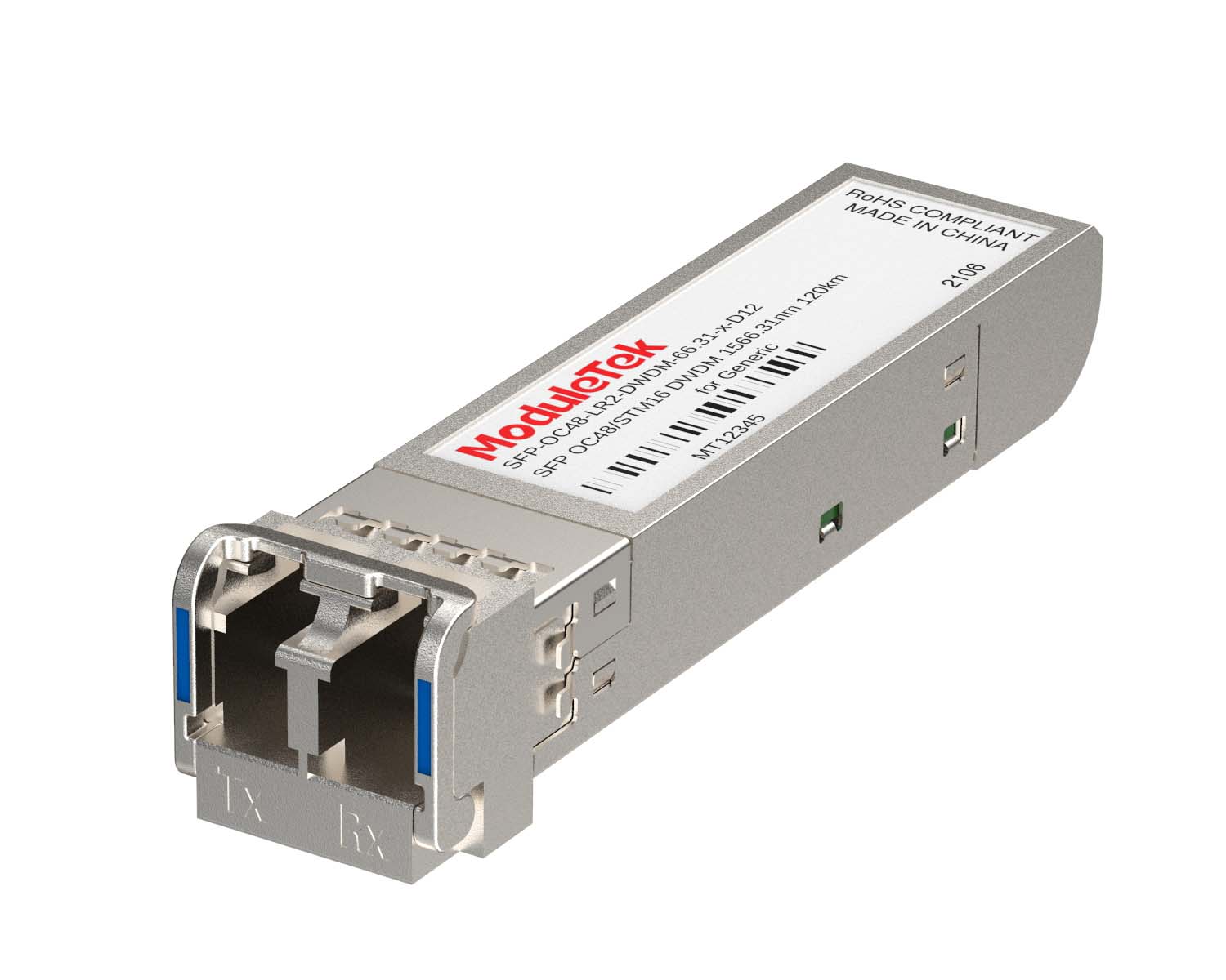 DWDM Optical Transceivers
 SGMII Port Optical Transceivers
 XFP Optical Transceivers
 100M/1G/10G Coppers
 Full-Rate AOC & Breakout Series
 10G/40G Active DAC Series
 Full-Rate Passive DAC Series
 40G/100G Passive Breakout DAC Series
 Regular/MTP-MPO Fiber Patch Cords
 MT2011
 MT2010
 CodingBox
 QSFP to SFP Adapter
 首页 > Home > Application Notes > Application Of Gold Wire Ball Bonding In Optical Module Manufacturing
Application Of Gold Wire Ball Bonding In Optical Module Manufacturing
Time: 2023-10-09
1. Introduction to Gold Wire Ball Bonding
Gold wire ball bonding, also known as gold wire bonding, is the mainstream process for internal wire interconnection in semiconductors. It is widely used in chip packaging for integrated circuits and interconnection between chips and external pins in active optical devices.
The working principle of common gold wire ball bonding equipment is as follows: under instantaneous high-voltage discharge, a tiny gold ball (also called FAB, Free Air Ball) forms at the end of the gold wire. Ultrasonic-frequency mechanical vibration is applied to bring the gold ball into contact with the surface of the material to be bonded, causing plastic deformation. With the assistance of ultrasonic energy, temperature and pressure, outer-shell electrons of metal surface atoms bond with each other to form a reliable joint.
There are four main internal factors affecting the bonding quality: ultrasonic power, temperature, bonding force and bonding time. External factors also play a role, such as gold wire gauge, bonding pad material, surface cleanliness of bonding pads, and wire routing shape.
In optical device manufacturing, 25 μm gold wire is commonly used for internal pin interconnection. This is due to gold’s excellent ductility (allowing fine wire drawing while maintaining sufficient tensile strength), electrical conductivity and solderability, which meet the precision processing requirements of communication semiconductors and high-quality electrical signal transmission.
2. Application of Gold Wire Ball Bonding in Optical Module Production
Gold wire ball bonding has two major applications in optical module manufacturing: TO-CAN packaging and COB (Chip-on-Board) processing.
2.1 TO-CAN Packaging
TO-CAN packaging in optical devices refers to mounting a bare die onto a TO header (usually made of gold-plated Kovar alloy) using epoxy adhesive or AuSn solder. Gold wire ball bonding is then used to interconnect internal chip pins and external pins on the TO header to form the target circuit. The die and bonding wires are protected via hermetic sealing.
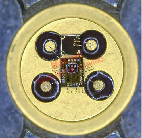
Figure 1 Schematic Diagram of Gold Wire Ball Bonding Inside TO-CAN
2.2 COB Processing
COB (Chip-on-Board) is a process in which a bare die is directly attached to a printed circuit board (PCB), followed by gold wire bonding and encapsulation to protect the die and wires. It offers superior signal integrity and has gradually become one of the mainstream packaging processes for high-speed optical modules.
Besides machine parameter settings, the PCB surface finish is another critical factor affecting gold wire bonding quality in COB processing. Currently, the preferred surface treatment for COB PCBs in the market is the NiPdAu (Nickel-Palladium-Gold) process. For more details about COB technology, refer to: Introduction To The COB Process For Optical Modules.
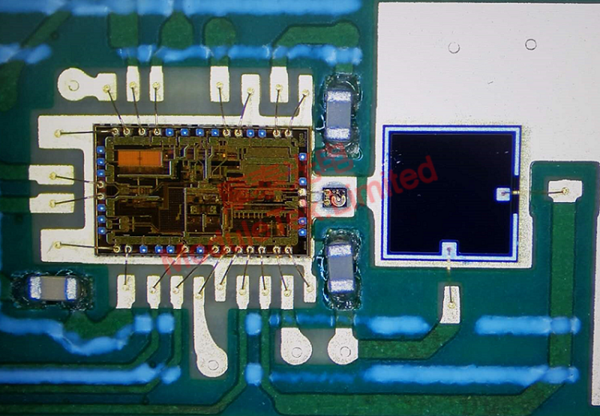
Figure 2 Schematic Diagram of Gold Wire Ball Bonding for COB in Optical Modules
Moduletek provides optical modules manufactured using gold wire ball bonding technology. Welcome to purchase!
For further inquiries about the above content, please contact us at: sales@moduletek.com