 40G/100G Optical Transceivers
 25G Optical Transceivers
 10G Optical Transceivers
 155M/2.5G Optical Transceivers
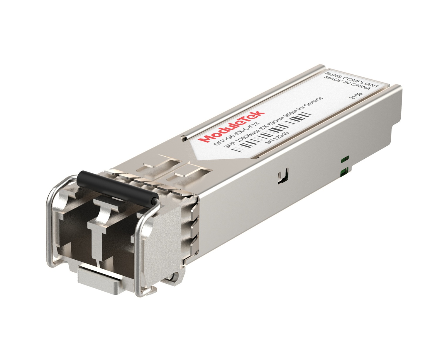 1G Optical Transceivers
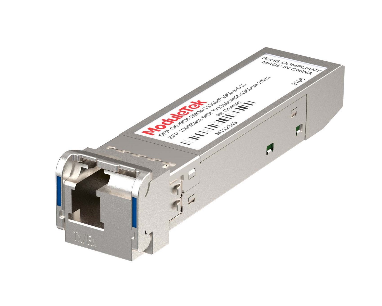 1G BIDI Optical Transceivers
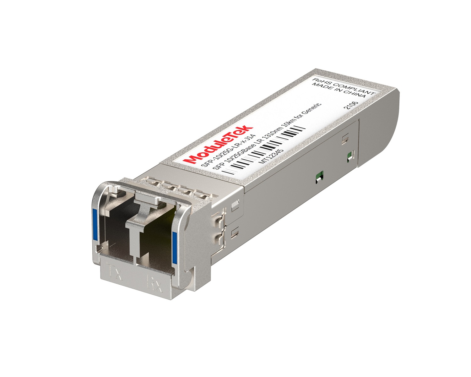 Dual-Rate Optical Transceivers
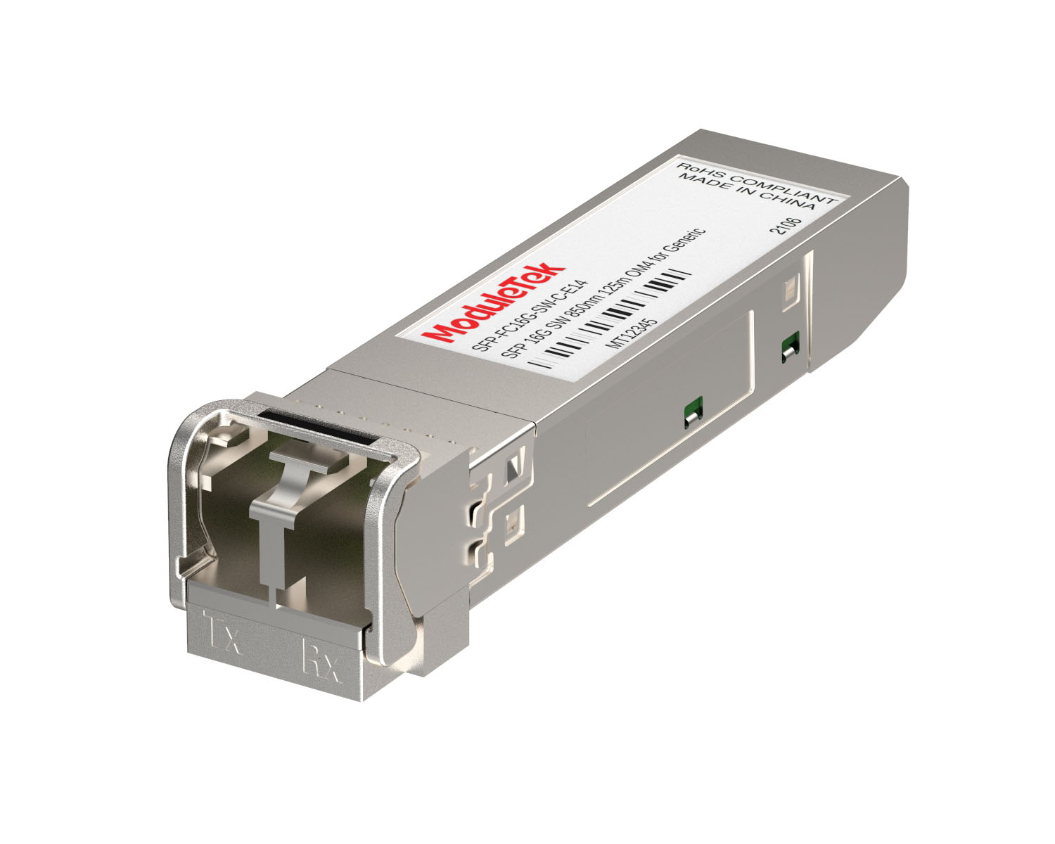 FC 16G/32G Optical Transceivers
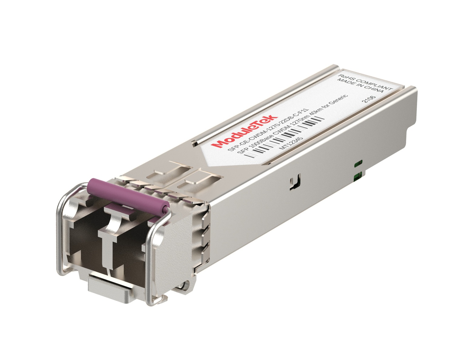 CWDM Optical Transceivers
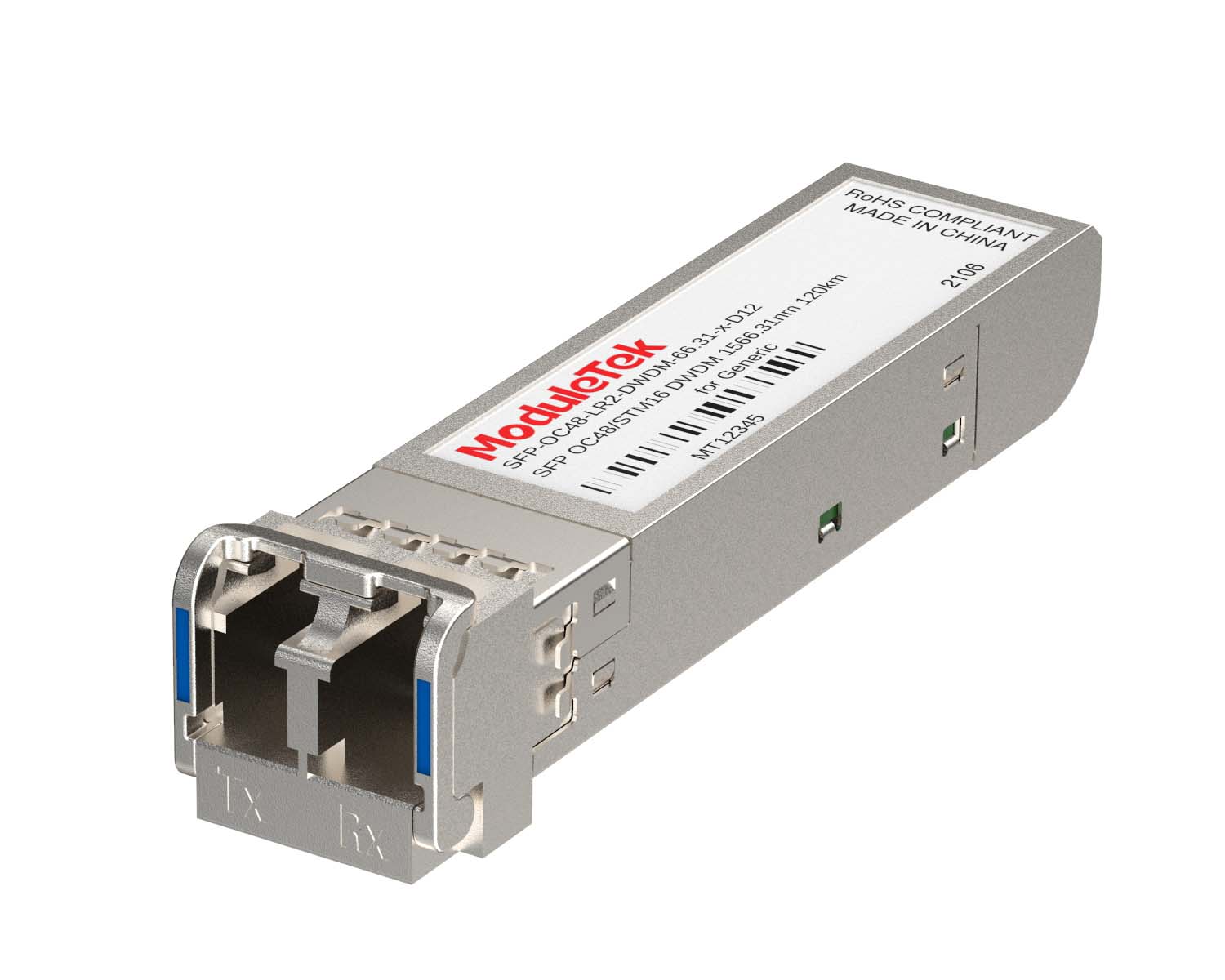 DWDM Optical Transceivers
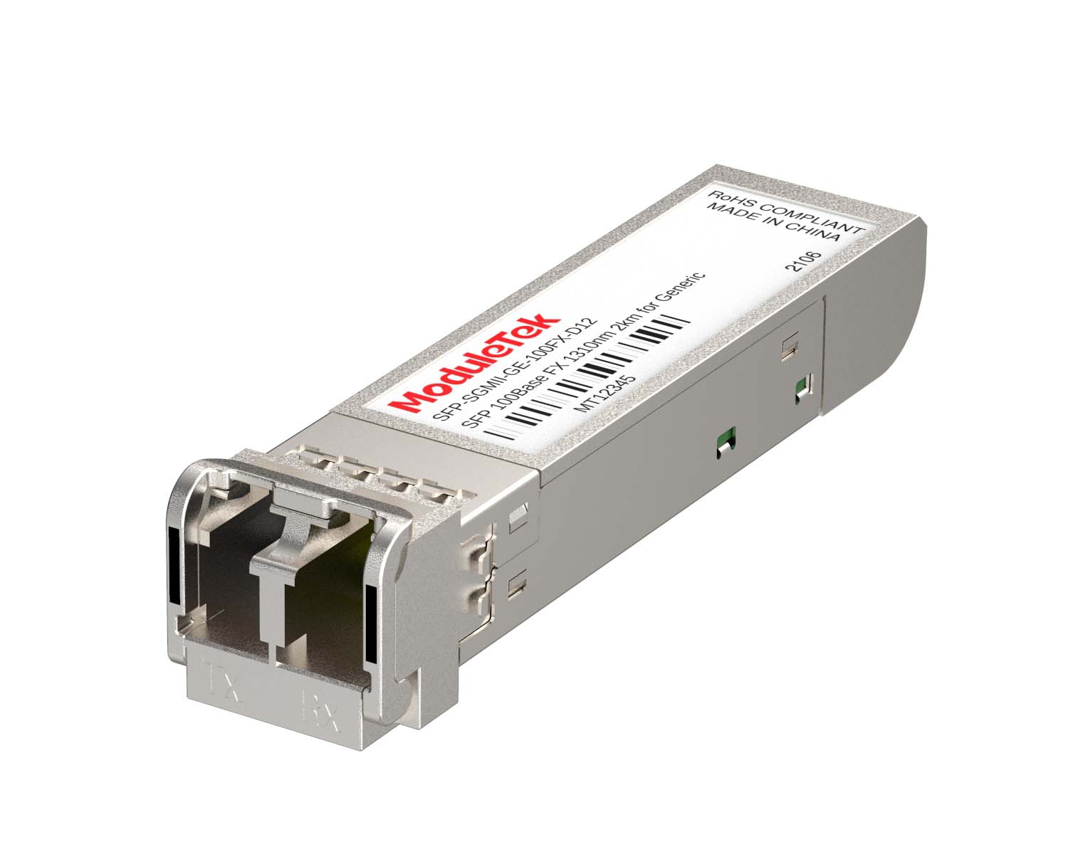 SGMII Port Optical Transceivers
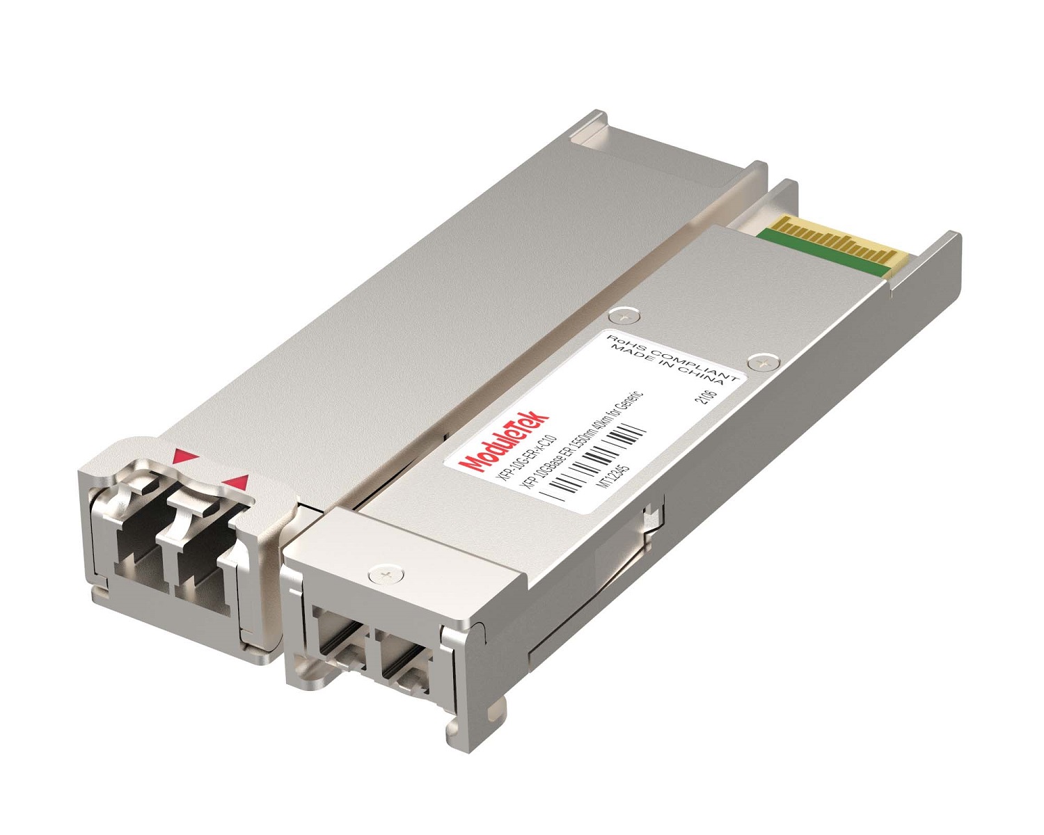 XFP Optical Transceivers
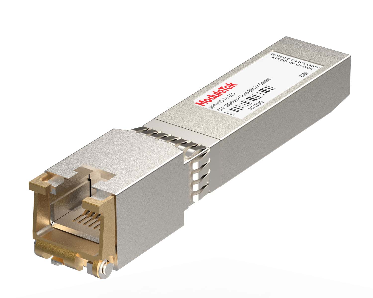 100M/1G/10G Coppers
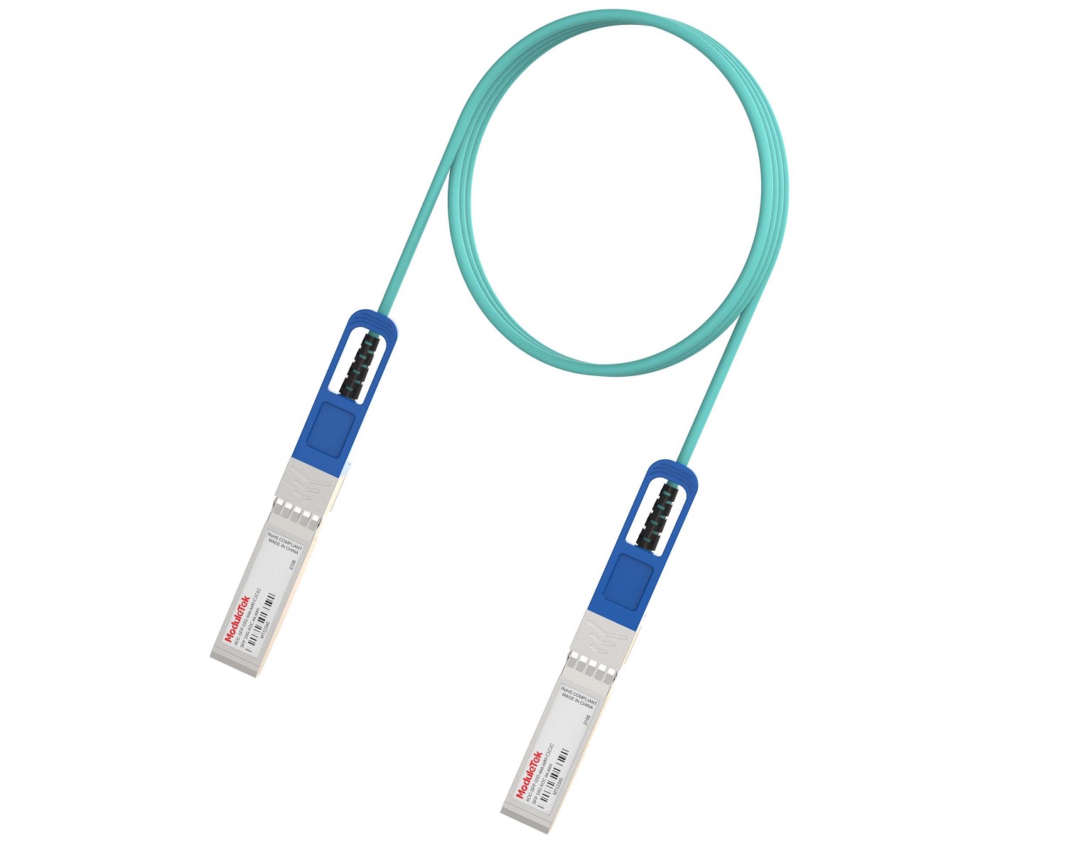 Full-Rate AOC & Breakout Series
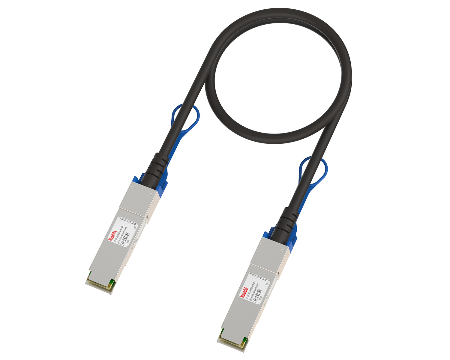 10G/40G Active DAC Series
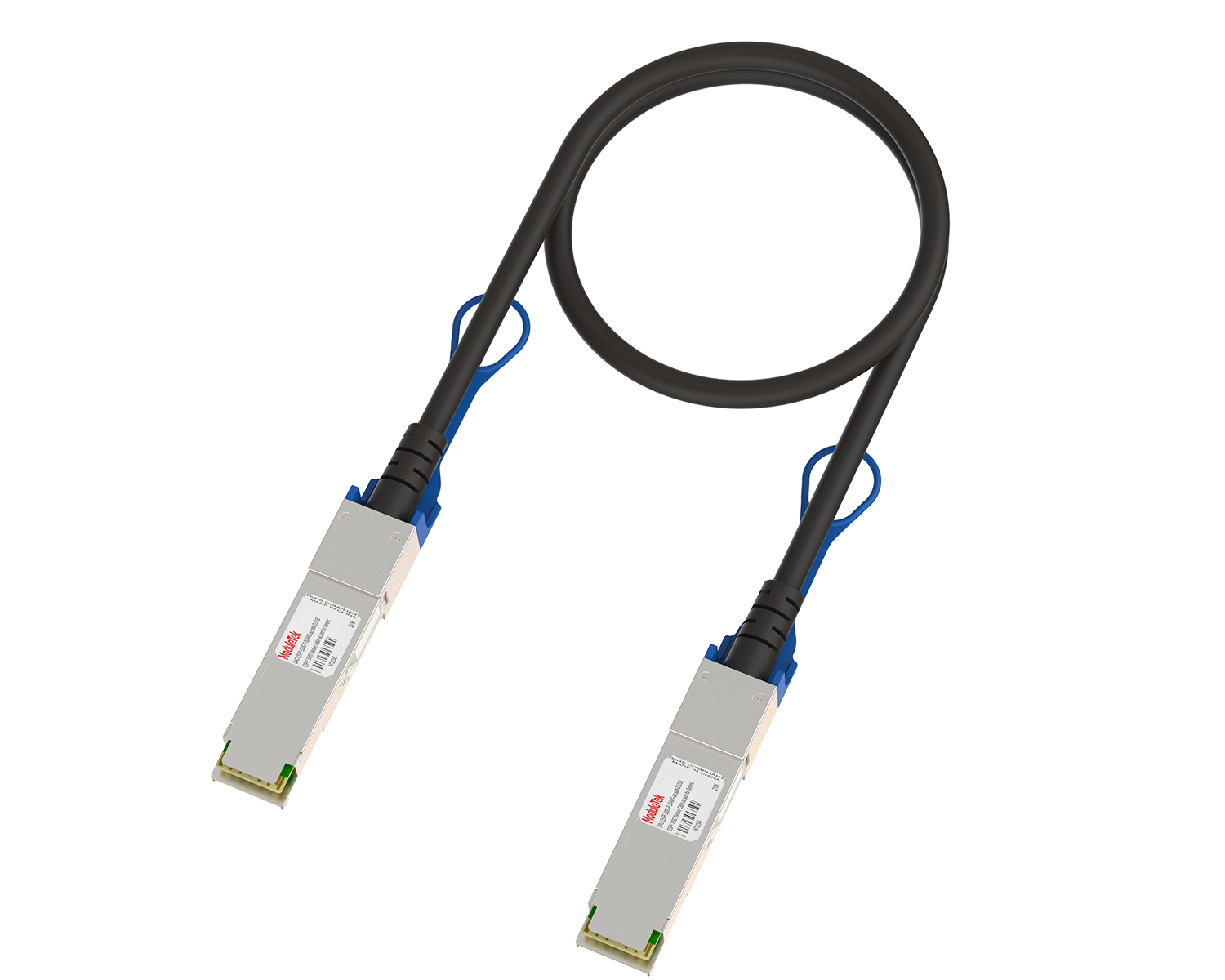 Full-Rate Passive DAC Series
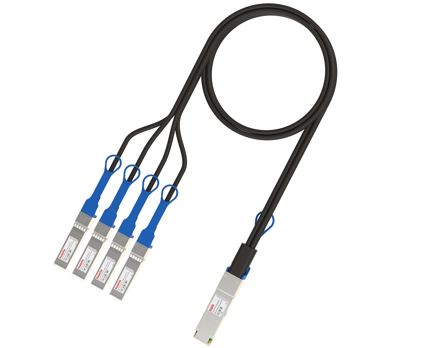 40G/100G Passive Breakout DAC Series
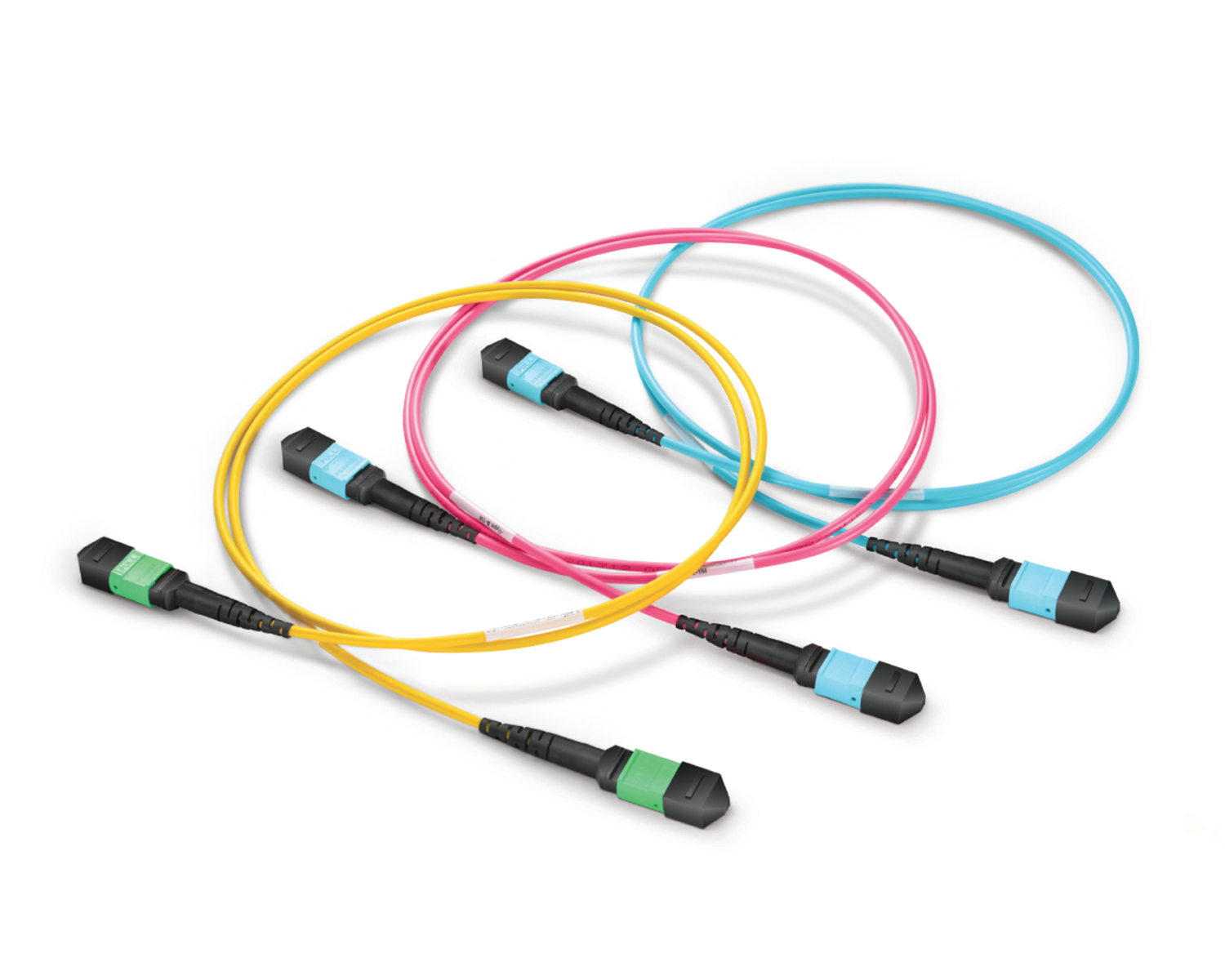 Regular/MTP-MPO Fiber Patch Cords
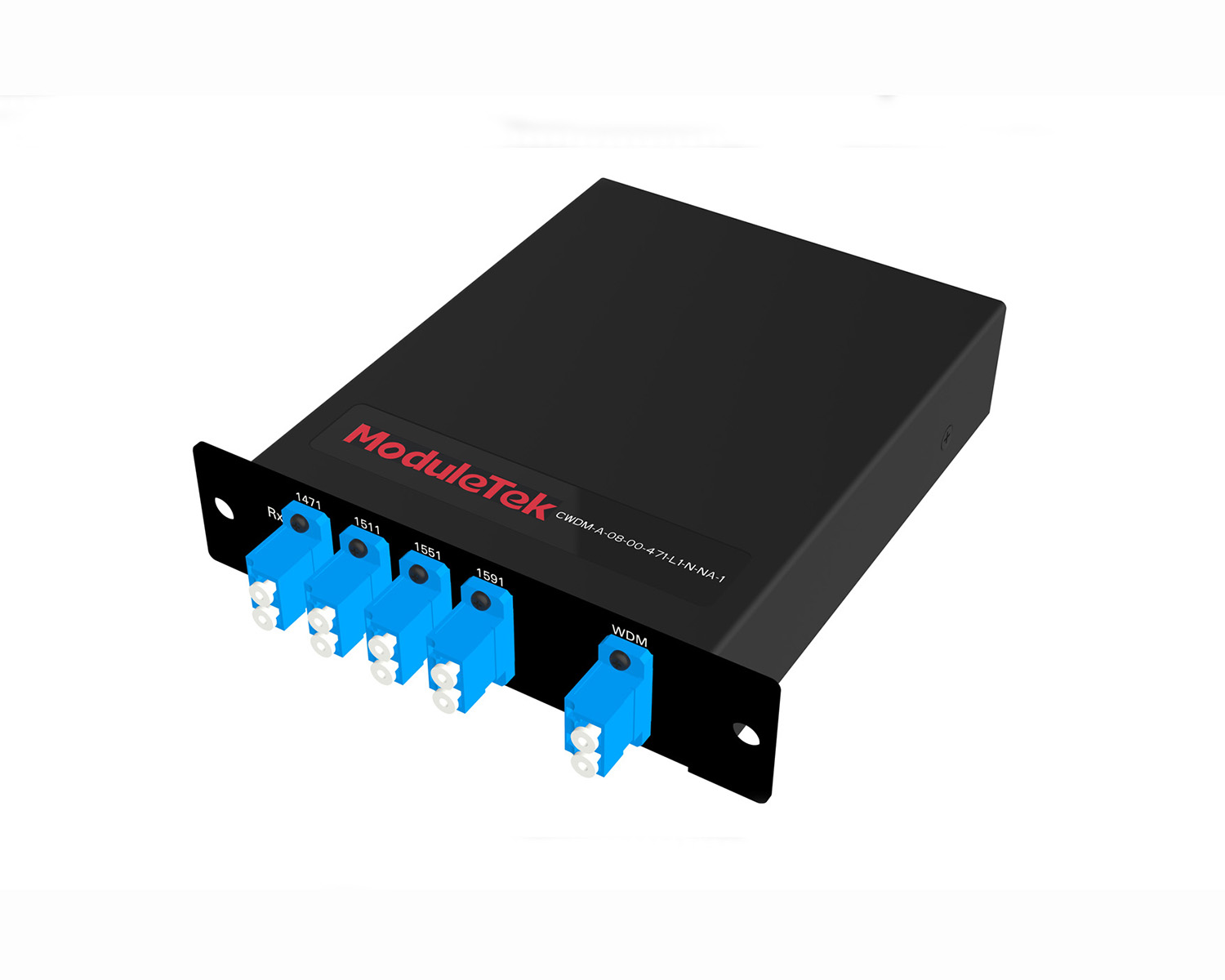 MT2011
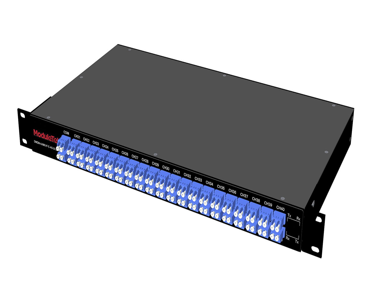 MT2010
 CodingBox
 QSFP to SFP Adapter
Electroless Nickel Palladium Gold (ENEPIG) Circuit Board Process
Time: 2019-02-26
Optical module products are trending toward miniaturization and high-speed operation. With the popularization of network communication, the demand for optical modules is constantly rising while their prices keep falling. To adapt to the miniaturization and mass production of optical modules as well as reduce costs, the Chip On Board (COB) production process has been introduced into the optical module manufacturing workflow. The COB process involves two key steps: first, directly mounting bare chips, lasers and other components onto circuit boards; second, achieving signal interconnection via gold wires through thermosonic welding usingwire bonding technology.
To meet the production and application requirements of optical modules manufactured with the COB process, circuit boards must satisfy the following criteria:
· The pads of the circuit board need to be plated with soft gold (pure gold) to enable fusion bonding with gold wires.
· The gold fingers of the circuit board must have excellent wear resistance to withstand repeated plugging and unplugging.
· The surface finish process of the circuit board should not be overly complex, which would otherwise lead to prolonged processing time and high costs.
· The process must comply with RoHS (Restriction of Hazardous Substances) requirements.
There are only two surface finish processes that can meet the above requirements for optical module circuit boards:
· Electroless Nickel Gold (ENEG) Process
This process involves electroless plating a layer of nickel onto the copper substrate, followed by a layer of soft gold on top of the nickel. Nickel is used because it exhibits good adhesion to both copper and gold. To prevent nickel from migrating to the surface through the micropores of the soft gold plating, which would contaminate and corrode the pads and cause bonding difficulties, the soft gold layer must have a certain thickness—≥ 0.3 μm. For the gold finger area, soft gold lacks sufficient wear resistance, so local hard gold plating (gold alloy) is required for this specific area.
ENEG also has an intractable production issue: wire bonding requires a gold thickness of over 0.3 μm, whereas soldering demands a gold thickness of around 0.05 μm to ensure good welding reliability. This requires area-specific gold plating thicknesses, which means separate surface treatments for the soldering, bonding and gold finger areas of the circuit board. The result is complicated processing procedures, high costs and low yield rates.
· Electroless Nickel Electroless Palladium Immersion Gold (ENEPIG) Process
Referred to as the nickel-palladium-gold process for short, this surface finish technology was originally developed by Intel. It adds a palladium plating layer between the nickel and pure gold layers, which isolates the nickel layer from the gold layer, thus preventing nickel migration to the surface gold layer. As a result, the thickness of the gold plating layer can be reduced to < 0.1 μm.
A 0.3 μm-thick palladium layer not only solves the gold finger wear resistance issue (thanks to its higher hardness than hard gold) but also acts as a barrier to prevent nickel migration. The entire circuit board can be processed using a single surface finish process—eliminating the need for area-specific plating steps—thus shortening the production cycle, improving the yield rate and reducing costs. Both palladium and gold are chemically stable metals, so circuit boards treated with this process have a long shelf life and can undergo multiple reflow soldering processes.
When the ENEPIG process was first developed, its cost was difficult to control because palladium was far more expensive than gold. However, with the decline in palladium prices, the current price of palladium isless than half that of gold. It is therefore an inevitable trend that the nickel-palladium-gold process will replace the nickel-gold process.
Table 1 Comparison of Characteristics Between the Two Processes
|
Characteristics
|
ENEG
|
ENEPIG
|
|
Shelf Life
|
Short (due to nickel migration)
|
Long
|
|
Processing Steps
|
Multiple gold plating steps (complex)
|
Palladium plating + gold immersion (simple)
|
|
Surface Gold Thickness
|
Thick (≥ 0.3 μm)
|
Thin (< 0.1 μm)
|
|
Wire Bonding Capability
|
Available (requires gold thickness ≥ 0.3 μm)
|
Available (only requires gold thickness < 0.1 μm)
|
|
Reflow Soldering Cycles
|
Unreliable
|
Reliable
|
|
Gold Finger Solution
|
Hard gold plating (wear-resistant)
|
Thick palladium + thin gold (wear-resistant)
|
|
Cost
|
High (thick gold plating)
|
Low (palladium is cheaper than gold)
|
|
Reliability
|
Low
|
High (palladium has good thermal diffusivity)
|
The circuit boards of Moduletek's SFP28 25G SR/AOC, QSFP28 100G SR/AOC, QSFP 40G SR/AOC products are manufactured using the nickel-palladium-gold process, ensuring excellent manufacturability. Welcome to contact us for product inquiries and orders.
For further inquiries about the above content, please contact us at: sales@moduletek.com


